VGA Basic / VGA Plus / VGA Professional
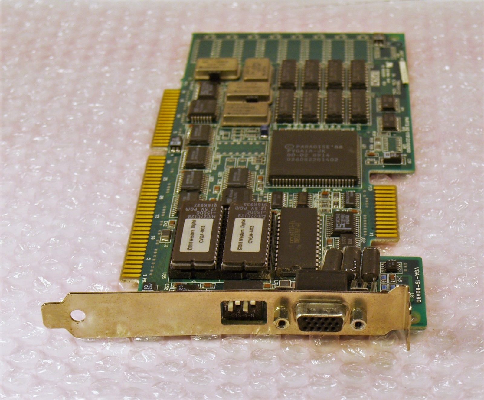
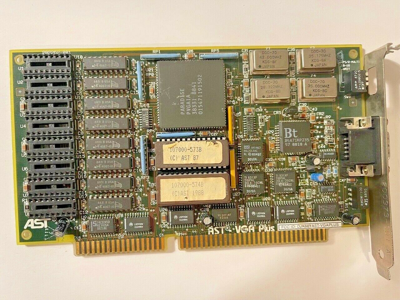
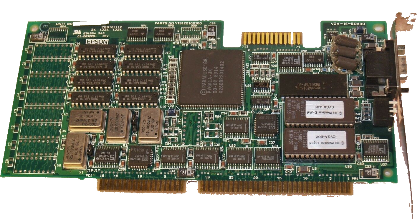
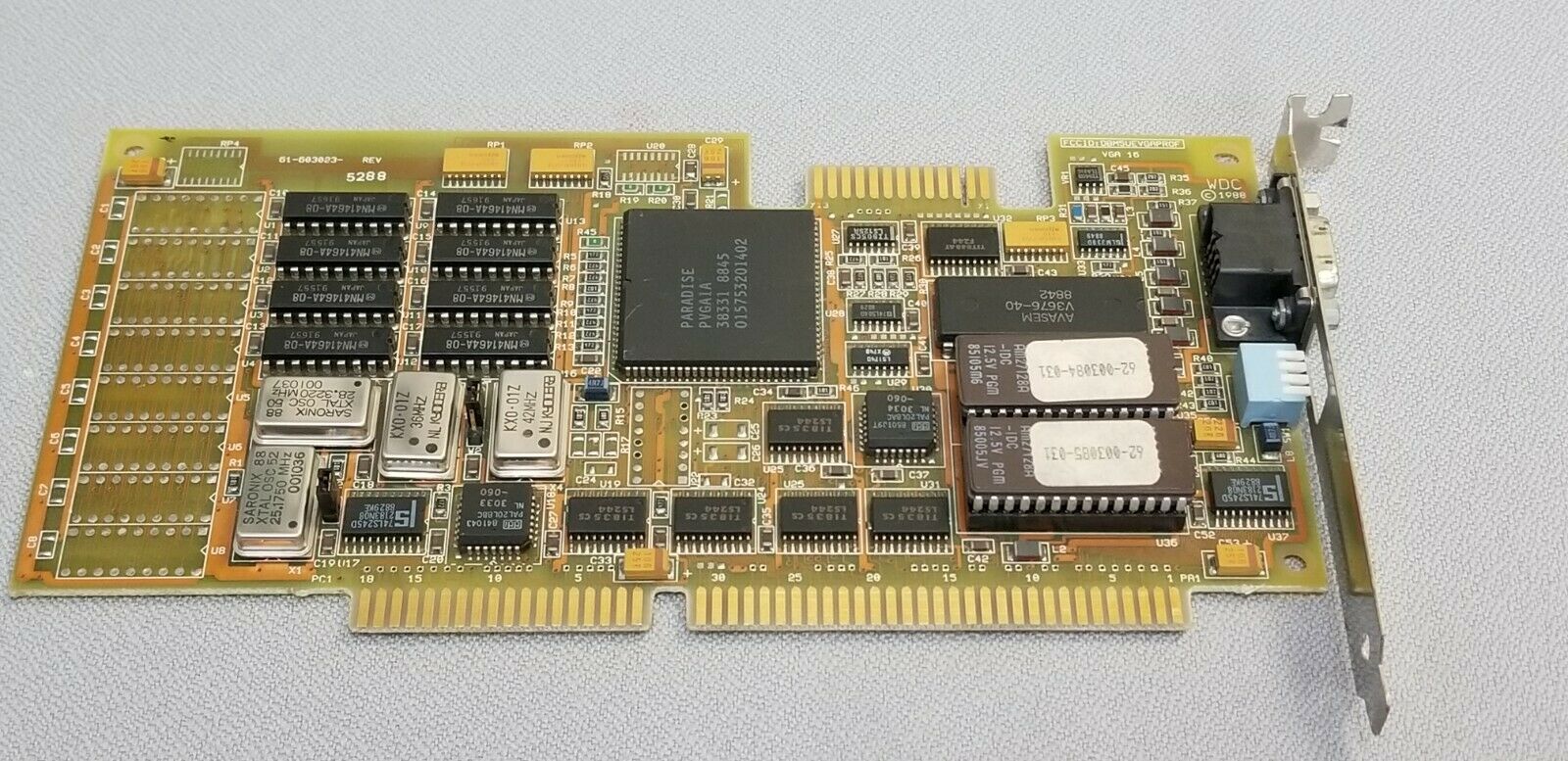
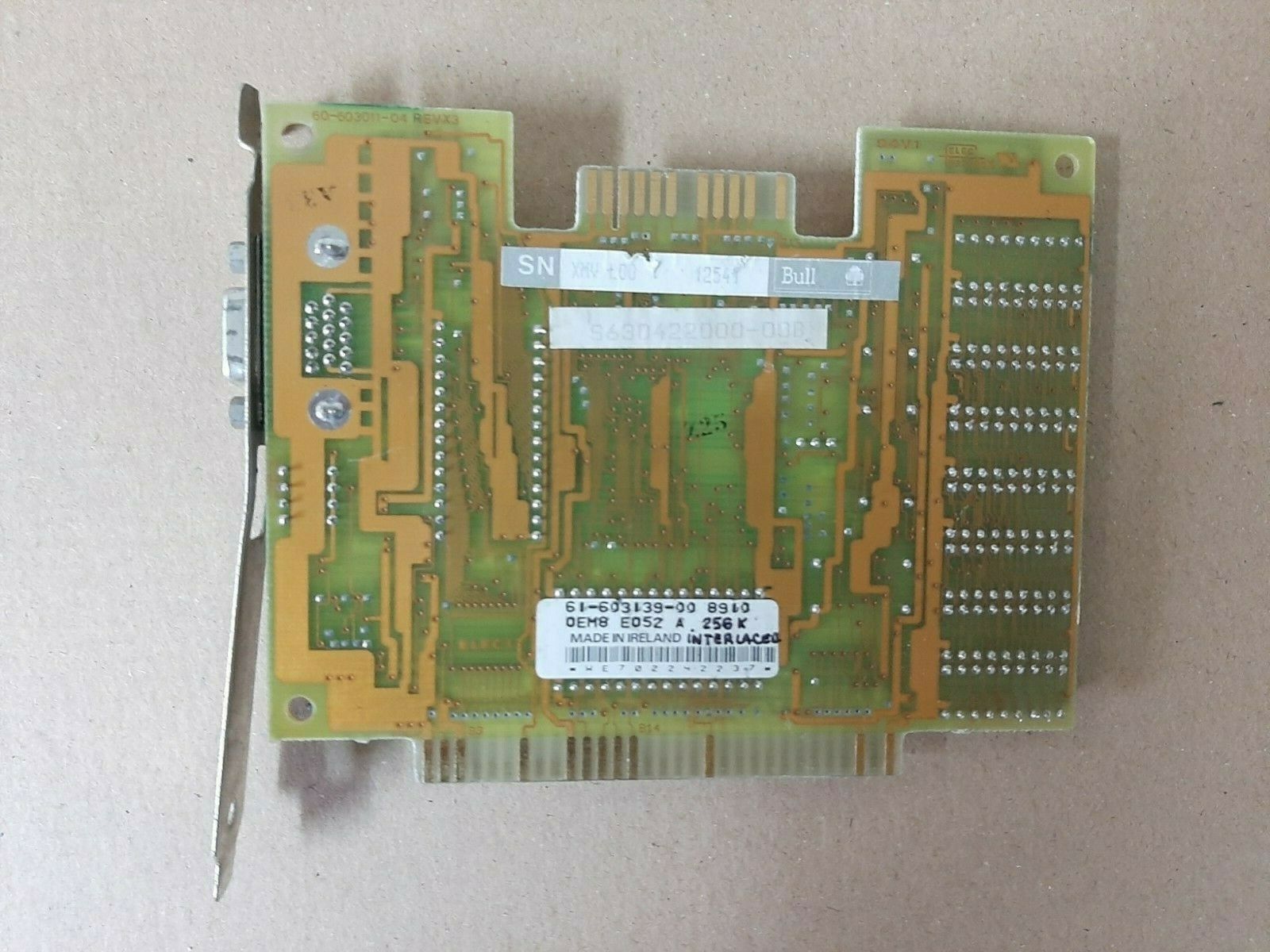
Paradise released three cards in 1988 based on the PVGA 1A chipset: The VGA Basic, VGA Plus, and VGA Professional. All cards used their new PVGA1A. The VGA Professional was a 16-bit card and came with 512 KB while the VGA Plus was the same card but with 256 KB onboard. The Basic VGA was the 8-bit offering with 256 KB onboard.
|
Released | 1988 |
| Bus | ISA 8-bit (Basic VGA), 16-bit (VGA Plus, VGA Professional) | |
| Chipset | PVGA 1A | |
| Standards | MDA, Hercules, CGA, EGA, VGA | |
| Memory | 256 KB (Basic VGA), 512 KB expandable to 1 MB (VGA Plus and VGA Professional). 16-bit data path, FPM DRAMs | |
| Ports | 15-pin DSUB (RGB analogue out) VGA Feature connector |
|
| RAMDAC | Inmos G171 or Brooktree (both 8-bit colour depth) | |
| RAMDAC Speed | 40 MHz (Inmos), 50 MHz (Bt) | |
| Part No. | 61-603011 (VGA Plus), 61-603023 (VGA Professional) | |
| FCC ID(s) | DBM5UEVGAPROF, BKME02V01, B948JAD1180A, DBM5VEPS2V00001 | |
| See Also |
The PVGA1A chipset from Paradise was a multi-mode VGA video controller with hardware and BIOS level compatibility. This means it provided 100% IBM VGA, EGA, CGA, MDA and Hercules graphics compatibility.
It supported a resolution of 640 x 480 in 256 colours as well as a 640 x 400 x 256 if 512 KB or more memory was installed (must be 100ns or faster), and a 42 MHz clock was installed (usually these cards come with a 36 MHz clock).
It added a non-standard 800 x 600 x 16 mode, which was supported by the game Wonderland. This mode requires a 240 KB frame buffer, but you most likely need a card with 512 KB of video RAM to support this mode.
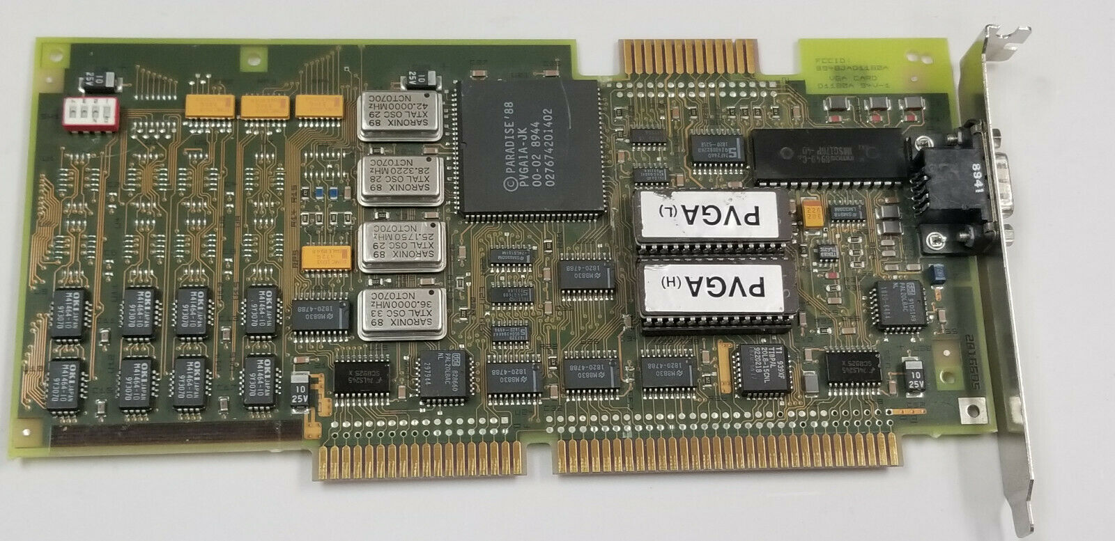
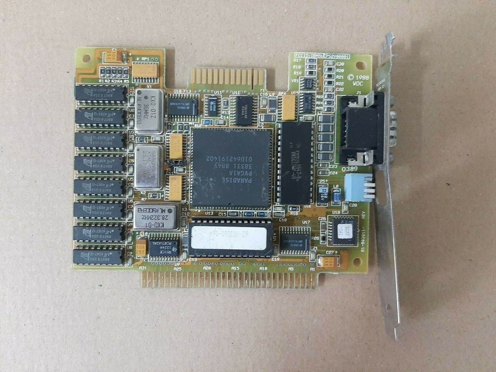
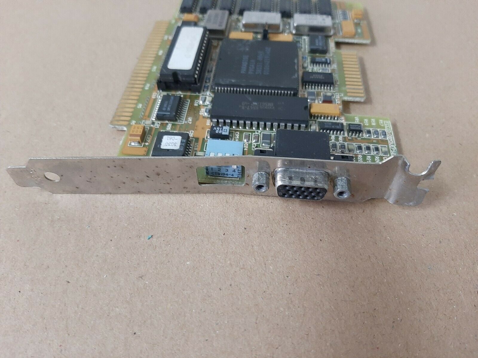
The PVGA1A chipset supports a video memory size of 256 KB, 512 KB and 1 MB. Cards that only have 8 DRAM sockets can only support 256 KB and 1 MB configurations, whereas 16-socket cards also supported 512 KB. This is because the three memory configurations that are supported are eight 64Kx4 chips (256 KB total), sixteen 64Kx4 chips (512 KB total), and eight 128Kx8 chips (1 MB total). The PVGA1A was packaged in a 100-pin PLCC or PFP.
Some cards based on the PVGA1A support 16 DRAMs while others have 8. Due to the way in which memory is organised, there are three memory configurations possible:
| Configuration | Total Memory | Maximum Resolution and Colours |
|---|---|---|
| Eight 64Kx4 DRAMs | 256 KB | 800 x 600 in 16 colours, or 640 x 400 in 256 colours |
| Sixteen 64Kx4 DRAMs | 512 KB | 1024 x 768* in 16 colours(?), or 640 x 480 in 256 colours |
| Eight 256Kx4 DRAMs | 1 MB | 1024 x 768* in 16 colours(?), or 800 x 600 in 256 colours |
So if you have only eight DRAM sockets on your card, it will not support 512 KB of video memory, only either 256 KB or 1 MB.
For my findings on the crystal oscillators on PVGA1A cards, see the section at the bottom of this page called Paradise/WD Crystals.
Paradise/Western Digital also shared the PVGA1A with Video 7 who marketed it as their VEGA chipset. After Western Digital's buyout of Paradise, the PVGA1A was rebranded as the WD90C00.
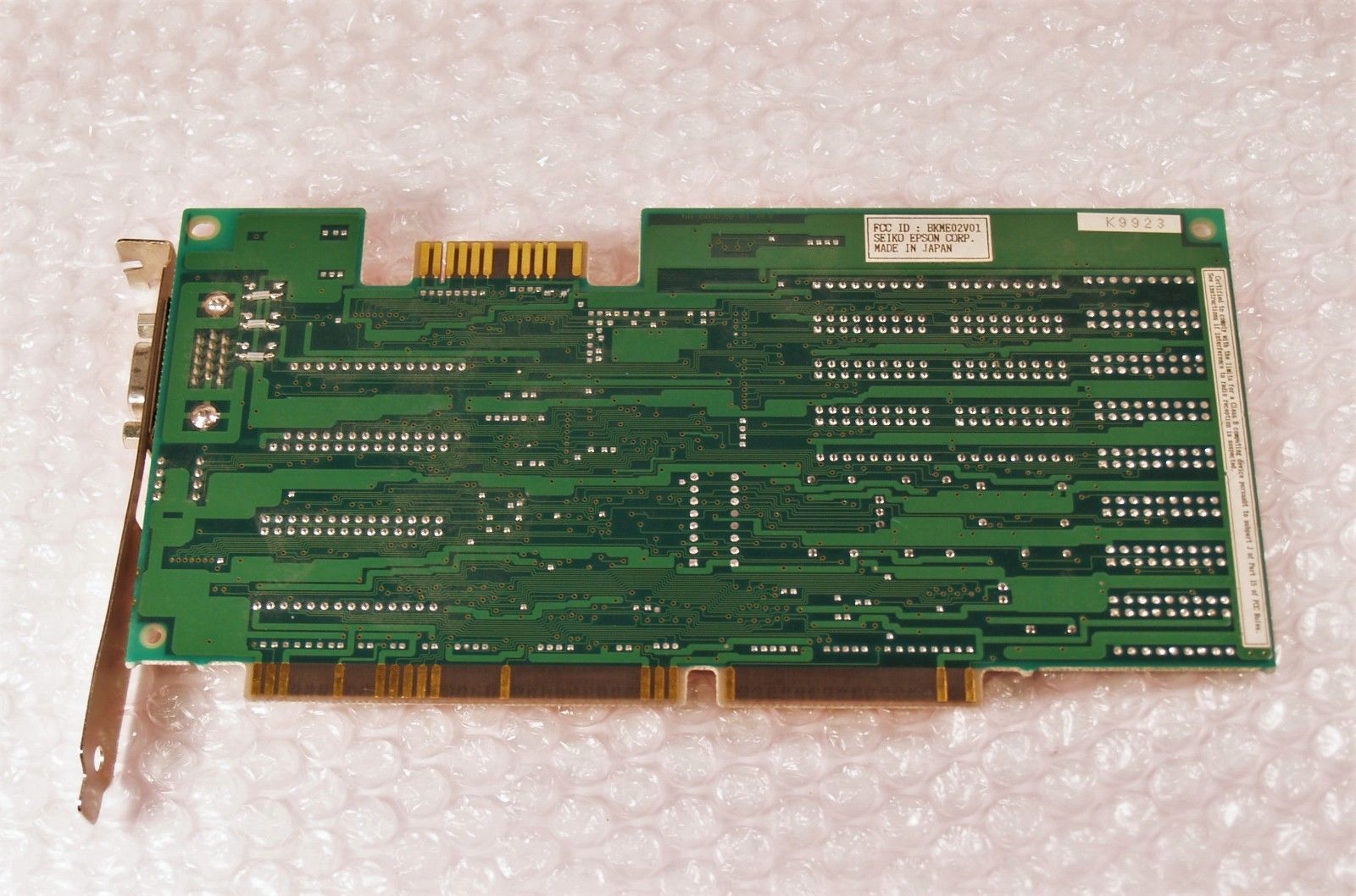
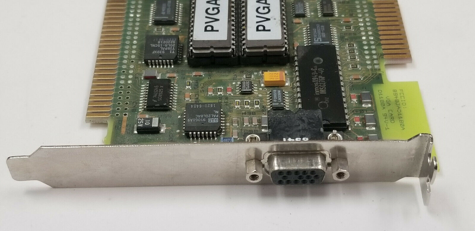
A Seiko/Epson-branded PVGA1A can be seen in the top image and first 2 images below, with FCC ID BKME02V01.
Row 2 is an HP-branded PVGA1A with FCC ID B948JAD1180A (presumably the model number is D1180A).
Row 3 is an AST VGA Plus MXB41.
Row 4 is a Philips card with FCC ID DBM5UEVGAPROF. This was also branded as the Expert TopVGA 2100.
Row 5 is a 256 KB Philips card with FCC ID DBM5VEP52V00001
Click here for the PVGA1A datasheet from October 1990.
Click here for another very similar PVGA1A datasheet (also from October 1990).
Paradise/Western Digital Crystals
Most Paradise and Western Digital SVGA graphics cards come with 3 or 4 crystal oscillators, which are defined as follows:
MCLK is the memory clock and determines the DRAM read/write access timing as well as the system CPU I/O and memory timing. MCLK should be 36 MHz if 120ns DRAMs are installed, and 42 MHz if 100ns or faster DRAMs are installed. This crystal should be of a higher value than VCLK0 and VCLK1.
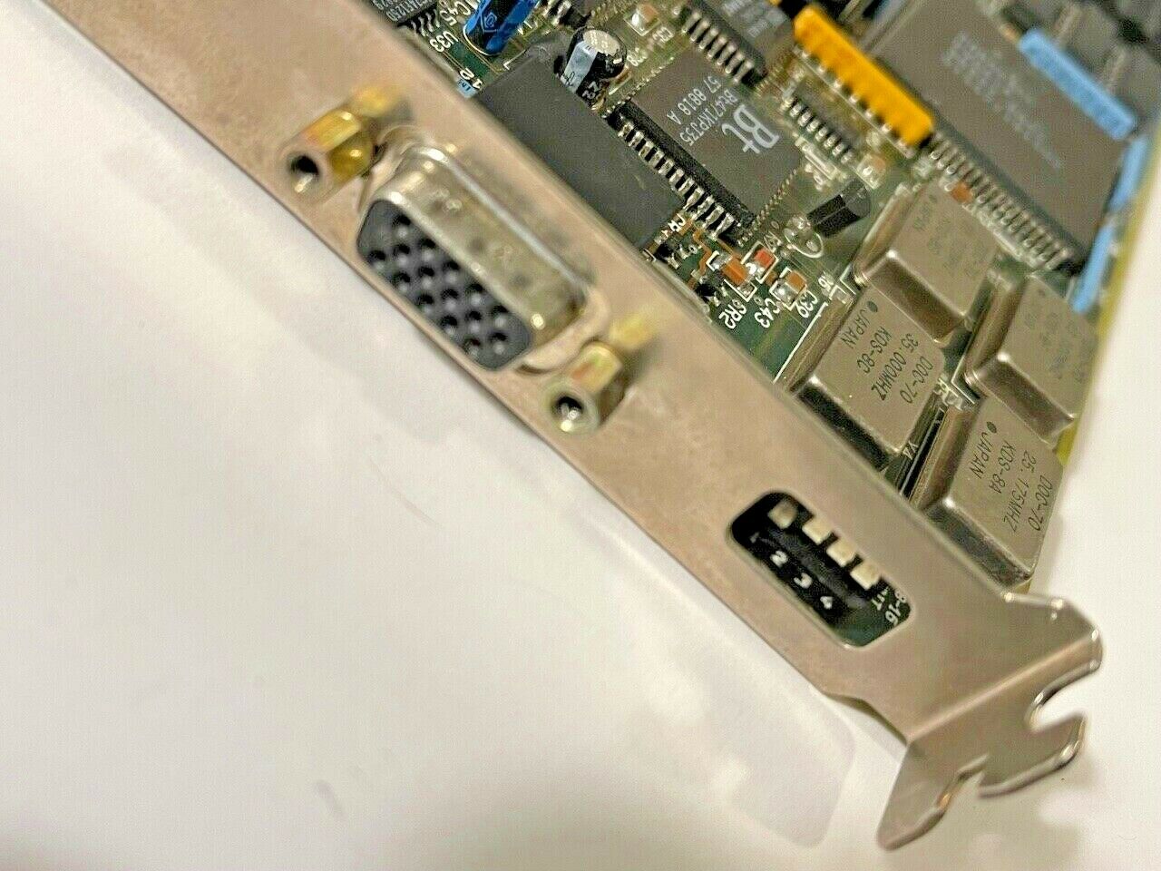
VCLK0 is the video display clock (aka, the dot clock) for both text and graphics modes. At 25.175 MHz, this displays 640 pixels per horizontal display line.
VCLK1 can either be a second video display clock input or an output to an external clock selection module. If used as an input, 28.322 MHz is used to display 720 pixels per horizontal display line.
VCLK2 (if a fourth crystal is present) can either be a third video display clock input, or an output to an external clock selection module. If present it is usually 42.000 MHz or 44.900 MHz - don't confuse VCLK2 with MCLK. If the card also has a 36 MHz crystal elsewhere, that one is likely to be your MCLK crystal, and the 42 or 44.9 MHz one would be VCLK2. Your card might have a jumper to enable this fourth crystal, i.e. VCLK2.
For 320 or 360 pixel modes, VCLK0, VCLK1 or VCLK2 is divided by 2 by the chipset to derive the pixel clock (PCLK).
Board Revisions
BIOS version 003056-007 is known to exist with a BIOS date of 07/14/88 on a VGA Plus.
BIOS version 003060-064 is known to exist on a VGA Plus.
BIOS version 003060-130 is known to exist (BIOS date sometime in 1989) on a VGA Plus.
BIOS version 003084-031 and 003085-031
are known to exist (odd and even ICs) on a VGA Professional
Competition
In the Media
Paradise Advert (1991)
Paradise VGA Plus Brochure
Paradise VGA Plus 16 Brochure
Setting it Up
Downloads
Operation Manual Get in touch if you can provide this missing item! |
Original Utility Disk Get in touch if you can provide this missing item! |
|
More Pictures
VGA Professional
VGA Plus

Another VGA Plus